GaAs - Alta
GaAs represents the highest level of PV technology because of its superior property and reliability. A traditional GaAs cell is expensive, heavy and fragile, and therefore cannot be applied to a mobile power system. The GaAs thin-film solar cell technology developed by Alta Devices is highly efficient, inexpensive, of superior power generation performance, lightweight and flexible, making it perfectly applicable to a mobile power system.
In Alta Devices, we grow epitaxial layers to form thin film solar products on a GaAs crystal chip by MOCVD and lift the device and flexible substrate off from the crystal chip by wet processing technology. Then products of different sizes are completed according to the customer’s needs. The MOCVD fast growing technology and VPE technology for large areas, developed independently by Alta Devices, allow large cost reductions and make large-scale manufacture possible.
GaAs - GSE
GSE adopts CIGS flexible co-evaporation technology. The production line uses a roll-to-roll technique to grow functional CIGS solar cells and films on flexible stainless steel substrates with a thickness of 30 μm; multipoint distributed evaporation sources are adopted to improve the evenness of films deposited; short evaporation process (less than 4 min.); raw materials are easy to acquire (Cu, In, Se particles, liquid Ga); double XRF are used to monitor the thickness and components of films deposited through co-evaporation and compensated by adjusting evaporation sources when off target; raw materials have a high use ratio, materials in the co evaporation hall can be recollected for reuse; easy dust management (changing the protection panel), and convenient evaporation source maintenance (6 hours maintenance).
In addition, GSE also owns an independent Integrated Cell Interconnect (ICI) packaging technique. The ICI packaging technique adopts image-based coating to produce electrodes featuring a tighter inner structure, having lowered the electric resistance of modules connected in series. Cells are connected via laser welding, which solves the issue of short circuits. The conversion rate loss of cells and modules has been largely reduced.
CIGS - Solibro
With 35 years of R&D and 10 years of real production experience, Solibro holds 88 patents and has demonstrated the integration and delivery experience of turnkey projects involving equipment-process-industry as well as integrated control of production costs.
The main technological features of Solibro’s CIGS co-evaporation technology: evaporation from the bottom up, multi-point source system and relatively large distance between sources and substrates. CIGS cell functional film coating is completed with different specialized devices. Advantages for industrialization: robust performance, great reliability, high production, convenient maintenance, high operation ratio and future efficiency and flexibility of technology improvement.
Today, Solibro is able to provide full support from a CIGS POWER LINE turnkey project customized design to the launch of a production line, including independent CIGS co-evaporation systems to ensure the high quality of a CIGS core process and the highest conversion rate.
CIGS - MiaSolé
MiaSolé adopts the world’s only CIGS one-stop automatic coiling magnetron sputtering coating system. It can complete the deposition of films for CIGS cells in vacuum conditions. A stainless steel substrate of eight kilometers long and one-meter-wide can be used once to produce 1.2MW of films.
Unique in-situ selenide technique and CdS sputtering coating technique shatters the yield rate and high cost ceilings of CIGS production.
Exclusive three-sided rotating comminuting and sputtering techniques; and rapid technique development.
Takt time less than 60 minutes; shortest R&D and manufacture cycle among the industry, 5% or less of normal takt time.
Environmentally friendly technique with no waste water or gas, featuring low energy consumption and meeting national environmental requirements.
The technology has received national attention with specified requirements of prioritizing development.
The Industrial Key Generic Technology Development Guide 2015 by the Ministry of Industry and Information Technology notes that “the R&D of CIGS cells production, especially the large-scale continuous roll-to-roll production technique, must be supported.”
HIT
Efficient silicon heterostructure technology refers to the heterojunction technology whose intrinsic layer has amorphous silicon material. The technology is to grow a total of 6 layers of film on both up and down surfaces of the n-type or p-type single-crystal silicon wafer. The structure of the double-sided SHJ cell of the Group is Ag gate / ITO film / p-type amorphous silicon film / intrinsic amorphous silicon film / n-type single-crystal silicon wafer / intrinsic amorphous silicon film / n-type amorphous silicon film / ITO film on the back / Ag grid on the back. An amorphous silicon film is only 5-10 nm thick and can be deposited using conventional cryogenic deposition techniques such as PECVD. The front and back of an ITO film can be produced by sputtering (PVD), with low industrialization costs. Due to the passivating effect of intrinsic an amorphous silicon film on the silicon surface, the reverse saturation current of the device is reduced by nearly two orders of magnitude, and the open circuit voltage and the PV conversion efficiency of the cell are greatly increased, achieving over 25% cell efficiency and over 23% module efficiency. High module efficiency saves BOS costs such as floor space, holders and labor costs. At the same time, the high open-circuit voltage leads to a lower temperature coefficient (-0.29%/°C) which enables better power output performance during actual power generation, about 6% more than conventional silicon devices. In addition, the double-sided symmetrical cell structure enables power generation of both sides. According to different ground conditions and different installation angles, this structure, under the same installed capacity, leads to 12-35% electricity compared to a single-sided silicon module, further reducing costs of power generation. The SHJ cell of the Group adopts an n-type single-crystal silicon wafer. Its modules do not have LID and PID in practical application with better environmental stability.
Product features: Cell conversion efficiency of more than 23%, stable module performance, low temperature coefficient, high output power under high temperature, service life of over 30 years, and substantial increase in electricity due to double-sided structure.
Target market: widely used in distributed power plants, BIPV, sound-insulating walls, agriculture/fishing, PV power generation at sewage treatment plants, mobile energy, among others.
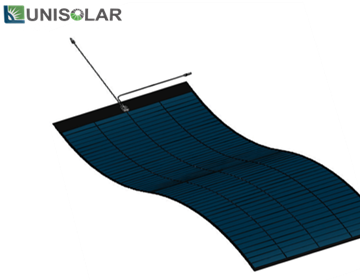
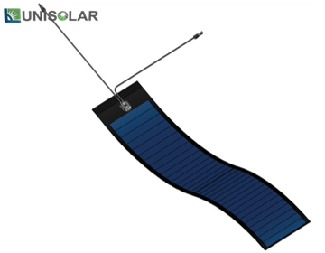
A-Si/Si-Ge
Both a-Si and Si-Ge are the non-crystalline allotropic form of silicon, and can be deposited as thin-films at low temperatures on a variety of substrates. They offer some unique properties for a variety of electronic applications. Despite lower electronic performance compared to multi-crystalline silicon (mc-Si), a-Si is much more flexible in its applications. For example, a-Si layers can be made much thinner than mc-Si layers, which may generate more savings on silicon material costs.
Another distinct advantage is that a-Si can be deposited at low temperatures (e.g. 75oC), not only on glass, but on inexpensive plastic as well, making it a candidate for a roll-to-roll processing technique. During deposition, a-Si can be doped in a similar way to mc-Si to form electronic devices. a-Si has become a core material and the active layer in thin-film transistors (TFT) used in liquid-crystal displays (LCD) and thin-film cells and modules.
Another advantage is that a-Si can be deposited over large areas through Plasma Enhanced Chemical Vapor Deposition (PECVD). The design of the PECVD system has a great impact on the production costs of a-Si modules. Therefore, most equipment suppliers focus on the design of PECVD equipment with higher throughput for lower production costs.
Through the technological breakthrough of an in-house developed Fab 2.0 Program on a tandem Si-Ge production line, the Group has achieved higher conversion efficiency, lowered production costs (reduced by 9%),and enhanced the cost-effectiveness and competitiveness of its thin-film power modules.
Nano-c-Si
Nano-crystalline silicon (nc-Si) has small grains of crystalline silicon within the amorphous phase. This is in contrast to mc-Si which consists solely of crystalline silicon grains, separated by grain boundaries. The difference comes solely from the size of the crystalline grains as most of the tiny crystallites of nc-Si are actually nanometer in size. Due to the presence of the silicon crystallites, nc-Si has a higher electron mobility than a-Si, which increases the absorption in the red and infrared wavelengths and thereby renders increased light-soaking stability over a-Si, making it an important material for use in Si thin-film PV cells. Similar to a-Si, nc-Si is a good choice for the active layer in thin-film transistors (TFTs), and thin-film PV cells and modules.
One of the most important advantages of nc-Si is its higher stability, making it easier to fabricate as it can be deposited using conventional low temperature a-Si deposition techniques, such as PECVD, as opposed to laser annealing or high temperature chemical vapor deposition (CVD) processes. By incorporating nc-Si into a-Si/a-SiGe to form a multi-junction solar cell, the cell efficiency can further be improved to 12% or greater, whereas the cost can be further reduced by 15% or more.